
SNES 2MB & 4MB PCB Adapters.
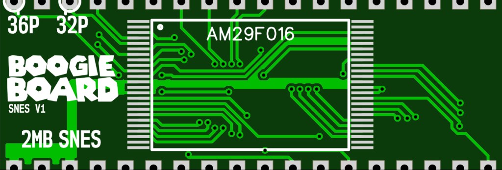
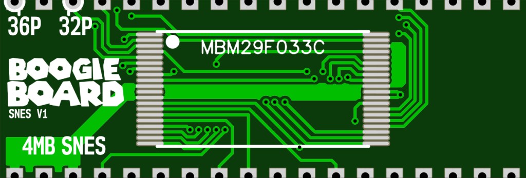
Table of Contents
- Introduction
- Section 1: Prerequisites and Materials
- Section 2: Dumping and Patching the ROM
- Section 3: Programming the EEPROM
- Section 4: Disabling the Factory MASKROM
- Section 5: Attaching the Boogie Board and Soldering the EEPROM
- Section 6: Troubleshooting and Tips
Introduction
Using this PCB adapter, an EEPROM, and some basic soldering, you can play translated or ROM-hacked games on genuine hardware. This step-by-step guide covers everything, from programming the EEPROM with the patched ROM to attaching the PCB and soldering it into the cartridge.
To preserve your game and ensure the modification is reversible, we’ll keep the original Mask ROM in circuit, allowing you to restore the cartridge to its original state at any time.
Please note that this tutorial is for educational purposes only and respects copyright laws. Make sure you legally own the original cartridge and ROM.
You can purchase both SNES Boogie Boards here at the shop.
Section 1: Prerequisites and Materials
Prerequisites:
- Method to Dump ROM: You’ll need a method to extract the original ROM from the game cartridge. There are various methods available, such as using a ROM dumper or cartridge reader. Familiarize yourself with the specific method you’ll be using.
- Translated Patch: Obtain a translated patch for the game you want to play. These patches are typically available online. Ensure that the translated patch is complete and compatible with the specific game you have.
- Basic Soldering Skills: Familiarize yourself with basic soldering techniques, as you’ll be soldering wires and components during the modification process.
Materials:
- Game Cartridge: To begin the modification process, you’ll need an original SNES game cartridge. This tutorial specifically focuses on modifying any 4MB or lower SNES/SFC game. However, it’s crucial to verify that your cartridge is compatible with this size
Keep in mind that patching a ROM can alter its size. If the applied patch exceeds the 2MB limit, the AM29F016 EEPROM will not be sufficient. It’s crucial to be aware of the ROM’s final size to ensure you select the appropriate EEPROM and adapter.
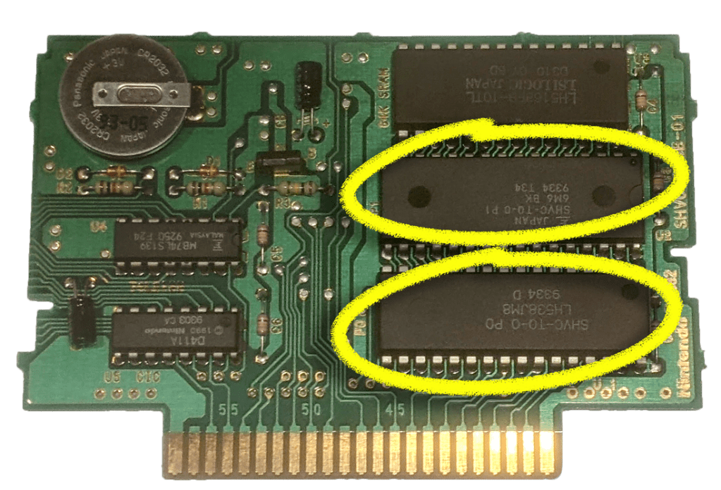
Additionally, it’s important to note that some SNES games utilize two Mask ROM chips. In these cases, the game’s data is split between the two chips. For example, you may come across a 4MB game that is divided into two 2MB Mask ROMs.
If you encounter a game that requires multiple Mask ROM chips, you will need to use two of my 2MB Snes Boogie Board adapters instead of a single 4MB board adapter.
It’s important to note that even for the same game title, different revisions may exist, resulting in varying PCB designs. Therefore, it is highly recommended to inspect your specific game board before proceeding. By personally examining the PCB and identifying its unique characteristics, you can accurately determine the number and type of Mask ROM chips involved. To gather more information about the PCB of your cartridge, I recommend utilizing a helpful website called SNESCentral. This website serves as a database of SNES circuit boards and offers assistance in identifying the components on your game’s PCB. It will aid you in understanding the composition of your game cartridge’s PCB. This knowledge will greatly assist you in selecting the appropriate Boogie Board adapters. - M29F033 or AM29F016 EEPROM: 5-volt, 32-megabit (4MB) or 16-megabit (2MB) non-volatile memory chip.
- 4MB or 2MB SNES Boogie Board: The SNES Boogie Board acts as the adapter for the EEPROM. It facilitates the connection between the EEPROM and the original Mask ROM’s pin out. Depending on the specific EEPROM you are using, you will need either the 4MB Boogie Board designed for the M29F033 or the 2MB Boogie Board designed for the AM29F016.
- Programmer: To program the EEPROM with the patched ROM, you’ll need a suitable EEPROM programmer. I highly recommend using the FlashcatUSB XPORT, along with the appropriate adapter for each EEPROM type. For the 4MB M29F033 EEPROM, you’ll need the TSOP-40 (Type-A) adapter, and for the 2MB AM29F016 EEPROM, the TSOP-48 (NOR X8) adapter.
In the “Preparing the EEPROM” section of this tutorial, I will provide a link to the FlashcatUSB XPORT, as well as the TSOP-40 and TSOP-48 adapters. - Wire: You’ll need a small amount of wire to disable the Mask ROM.
Section 2: Dumping and Patching the ROM
This tutorial will not cover ROM dumping in detail but it is worth mentioning. In this section, I will mention a few devices that will dump ROMs from the SNES cartridge. I know its not the most common method, but I use a modified Retron5.
2.1 ROM Dumping
If you are a weirdo like me and own a Retron5 console, you can refer to the tutorial by ezgoodnight on retrorgb.com to install RetroNFreak 2.5 on to your Retron5. This Custom Firmware (CFW) will enable you to extract the ROM directly from your SNES game cartridge and save it onto an SD card, but there is a catch. Even if you install the CFW on your Retron5, the ROM dumps you create will be encrypted. As a result, it makes the whole thing pointless. The dumps will not work on anything other than your Retron5. If you want to use a Retron5 for this tutorial, you will need to decrypted the ROMs. Luckily on jonasrosland’s github there is a way to modify the Retron5’s external SD card to obtain decrypted ROMs. Just following the instructions they provided in the link here. Its a lot of work to obtain something you already own, but it’ll get the job done. If you don’t have a Retron5, or if you’d prefer an easier method, don’t worry—I’ll cover another way to dump ROMs later in this section. You might also find some helpful “resources” to “download” elsewhere online (wink, wink).
After all that unnecessary hassle, dumping the ROM with the custom firmware installed is simple: just insert the cartridge and confirm that you’d like to install the game. Done.
An alternative method for dumping ROMs is the Sanni Cart Reader. It’s an Arduino-based, open-source project, and all the information you need to build your own cart reader is available on Sanni’s GitHub. If you lack the technical skills to build one yourself, you can check out Save the Hero Builders. As of this writing, they offer Hardware Version 3 of the Sanni Cart Reader for purchase.
2.2 Fixing Checksums/Removing Header
Before applying the patch, I want to cover how to properly check the ROM. For this purpose, we will be using uCON64.
This command line utility provides detailed information about your ROM. Follow the steps below to get started:
- Create a Work Folder: To make it easier to organize your work materials, I recommend creating a dedicated folder where you can store all the necessary files and tools.
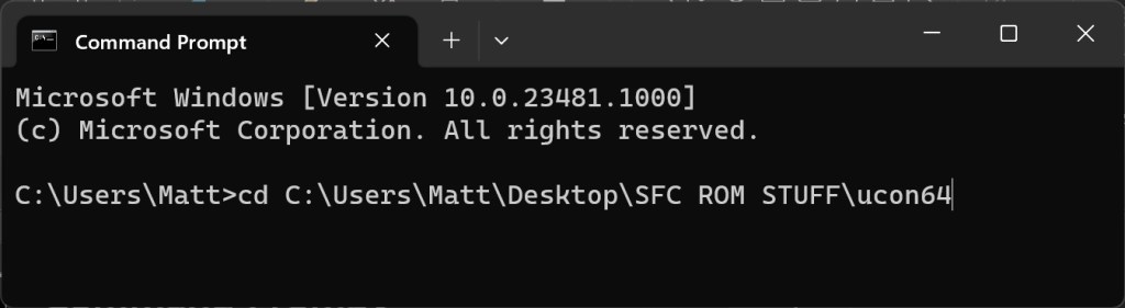
- Download and Unzip uCon64: Obtain the uCon64 program and unzip it to a location of your choice on your computer. Make note of the folder where uCon64 is located.
- Open Command Prompt: Launch the Command Prompt application on your computer. To change the directory to the folder where uCon64 is located, use the cd command. For example, if uCon64 is located on your D drive, the command would be:
cd D:\path\to\uCon64-folderAlternatively, you can navigate to the folder manually in File Explorer, type “cmd” in the beginning of the address bar, and hit Enter. This will open Command Prompt with the directory set to the folder you’re currently in.
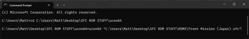
4. Locate Your ROM: Navigate separately to the location where your ROM file is stored. Hold the Shift key, right-click on the ROM file, and select “Copy as path” from the context menu.
5. Paste the ROM Path: Switch back to your Command Prompt window and enter the following command:
ucon64 [path to ROM]Use CTRL+V to paste the path you copied in the previous step. Hit Enter to execute the command.
6. View the ROM Information: After executing the command, uCon64 will provide you with a wealth of information about your ROM file. Take the time to review the details displayed on the screen.
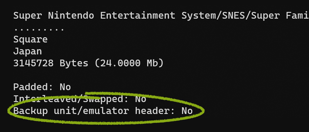
By following these steps, you’ll be able to use uCon64 to get info on the ROM from your SNES game cartridge. In the next subsection, we’ll cover what some of the info means but primarily checking to see if the ROM is headerless and the checksums are good.

- Region: The ROM must be for the correct region’s color encoding system, either PAL or NTSC. The PAL region operates on 50 Hz , while the NTSC region operates on 60 Hz. Using a ROM intended for the wrong color encoding system can result in games running poorly or not at all.
- Padded: the act of adding extra data or bytes to a ROM file in order to meet a specific size requirement. ROM files often have predetermined sizes based on the type of cartridge or storage medium they are intended for. When a patch modifies a ROM and increases its size slightly beyond the expected amount, padding may be required to align the data correctly within the ROM’s structure. For example, let’s consider a scenario where the original game ROM is 1MB in size, and after applying a translation patch, the ROM size increases to 1.2MB. In order to ensure compatibility with real hardware, the ROM will need to be padded to the next expected size, which, in this case, would be 2MB. It’s important to note that padding is typically not necessary for SNES/SFC ROMs. These systems often have flexible memory mapping that can accommodate different ROM sizes. However, for NES/FC ROMs, padding becomes crucial. NES/FC ROMs have stricter memory requirements, and padding ensures that the ROM data aligns correctly with the memory banks and addressable space. It’s worth mentioning that some SNES/SFC games are designed to work with specific ROM sizes as a form of copy protection. If the ROM size being used is smaller than what the game expects, issues can arise during gameplay. An example mentioned is Final Fantasy V (FF5), which needs to be padded from 24 Mbit to 32 Mbit. If the ROM size is not padded to the expected 32 Mbit, a black screen with music will be displayed after pressing start at the beginning of the game.
- Interleaved/Swapped: a technique where the bytes or data within the ROM are rearranged or reorganized in a non-sequential manner. This can be done for various reasons, such as optimizing data access or providing a specific structure required by the hardware or game system. The “Interleaved/Swapped” information indicates whether the ROM data follows a specific interleaving or swapping pattern. This information is useful when working with ROMs that have a non-standard organization or when troubleshooting issues related to the ROM structure. In the context of Sega Genesis ROMs the ROM data is arranged in a specific way where the bytes are swapped or interleaved to match the Big Endian byte order required by the Sega Genesis hardware. This byte swapping ensures that the data is correctly interpreted by the processor of the Sega Genesis console.
- Backup Unit/Emulator Header: a specific type of header information found in ROM files. This header provides information related to backup units or emulation settings. For example, some ROM files may contain a header that specifies the type of backup unit used to save game progress, such as a battery-backed RAM or flash memory. This information is useful for emulators or backup devices that need to simulate the functionality of the original hardware’s backup unit. Additionally, the header may include emulation-specific settings or flags that control how the ROM is handled by emulators. These settings can affect various aspects of the emulation, such as audio, video, input, or other system-specific features. Headered ROMs are not needed on real hardware. The header information typically serves purposes related to emulation, backup units, or specific software requirements. Real hardware usually does not rely on or recognize the header information.
- Bank Type: The ROM can be categorized into two main types: HiROM and LoROM. HiROM games are indicated as “HiROM: Yes” in the command window, while LoROM games are indicated as “HiROM: No”. This information determines the memory mapping used by the game. HiROM (High-ROM) is a memory mapping scheme where the ROM data is organized in a certain way to access the higher address range of the SNES’s memory. HiROM allows access to the upper half of the SNES’s memory space, while LoROM accesses the lower half. The distinction between the two is based on how the ROM data is banked and accessed by the SNES hardware.
- ROM Size: This indicates the size of the game’s ROM. It is essential information when selecting the appropriate chips for programming the game. Most cartridge boards can handle games of various sizes, so it is crucial to choose chips that can accommodate the specific ROM size.
- ROM Type: This section lists any specialty chips used by the game. It excludes default chips found in all games, such as the CIC region chip or ROM chips. For example, some games use specialized chips like the Super FX chip. Additionally, certain games may require batteries for functions like game saves. It’s advisable to replace these batteries, even when converting an older cartridge to a different game, as the original batteries may be nearly dead after several decades.
- Speed: This refers to the data access delay times of the ROM. In most cases, you can disregard this information as EPROMs and EEPROMs available today are typically fast enough for both types of games. If you want to ensure compatibility, check the datasheet of your chip and ensure that it specifies at least 120 ns access time.
- SRAM: Some games utilize SRAM (Static random-access memory) to save game progress or data. It’s important to provide the game with the exact amount of SRAM it requires. Some games perform checks to ensure that the available SRAM matches a specific amount.
- Checksums: verifies the integrity of the ROM’s actual data. uCON64 calculates a checksum value for the ROM’s data sections (excluding the header) and compares it to the expected checksum value. If they match, it indicates that the data is intact and has not been corrupted. By comparing the calculated checksum values with the expected values, uCON64 can detect any inconsistencies or modifications in the ROM file. If the checksums do not match, it suggests that the ROM file may be corrupted, modified, or incompatible with the expected format. When you apply a patch to a ROM, it alters the data, such as replacing text or modifying code. As a result, the checksums associated with the ROM may no longer match the expected values, as they were calculated based on the original unmodified ROM.
You ran ucon64 and see Bad checksums, now what?
If your checksums are bad, you can use a program called IpsAndSum to fix them. It’s a bit glitchy but easy to use.
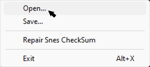
1. Open IpsAndSum and go to File > Open to select your ROM.
2. The numbers on the screen may change or stay at 0000, don’t worry about it.
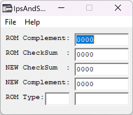

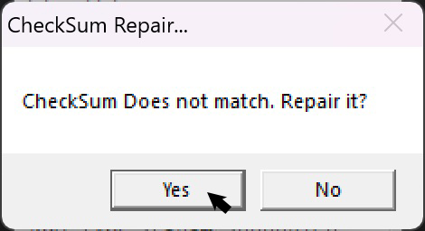
3. Next, go to File > Repair SNES CheckSum. The fields should update.
4. Click “Yes” to repair the checksums.

5. Finally, go to File > Save to save the fixed ROM.

After fixing the checksums, it’s a good idea to run the ROM through uCon64 again to double-check if the checksums are now fixed. Also, remember to save the ROM by going to File > Save (It’s easy to forget).
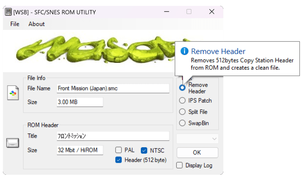
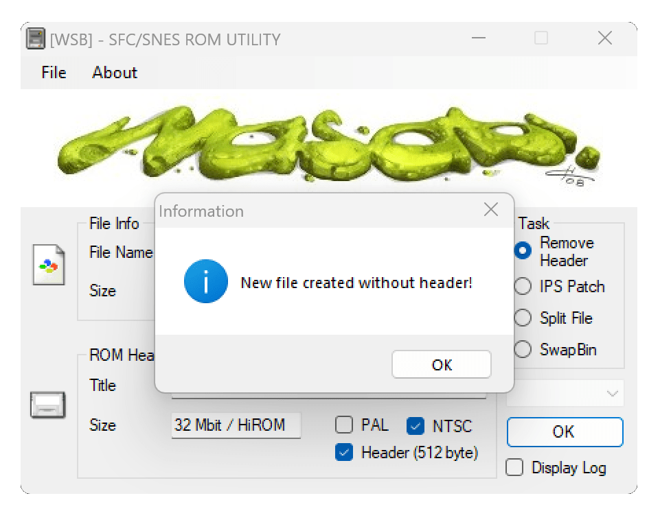
Your ROM has a header and you need to remove it. Here is how.

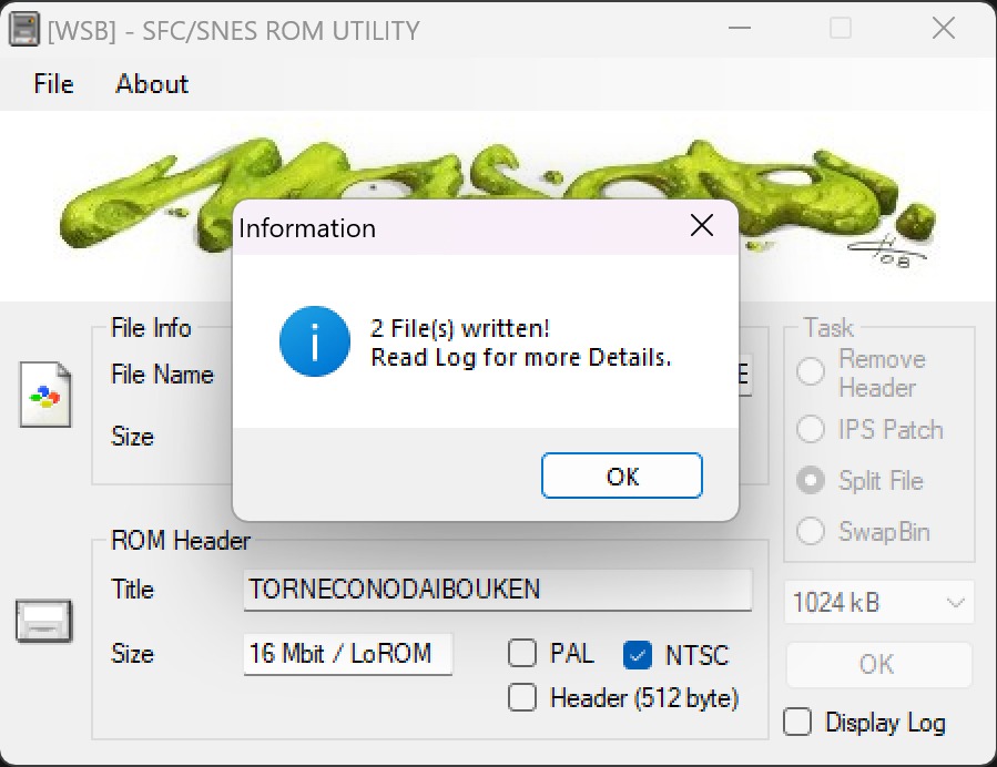
We will use a program called SNES ROM Utility to easily remove the header.
- Simple load the ROM under File > Open
- Check “Remove Header”
- Hit “OK”
2.3 ROM Patching
Translated Patch: Once you have successfully dumped the original ROM from your game cartridge, it’s time to apply the translated patch. Numerous online resources offer translated patches for a wide range of SNES games. Find a reliable source that provides the translated patch for your specific game and download it.
- Patching Tools: Online ROM patching tools simplify the process of applying patches to your ROM. Typically, these tools require you to upload your original ROM and the translated patch. The tool will merge the patch with the ROM, resulting in a patched ROM. Follow the instructions provided by the specific patching tool you choose.
- Verify Compatibility: Ensure that the translated patch is compatible with your dumped ROM. Some patches may be designed for specific versions or regions of the game. Check the patch’s documentation or online resources to confirm compatibility.
- Apply the Patch: Use the online patching tool to apply the translated patch to your dumped ROM. This process usually involves uploading both files (original ROM and patch) and initiating the patching process through the tool’s interface. Once the patching is complete, you’ll have a new ROM file that contains the translated version of your game.
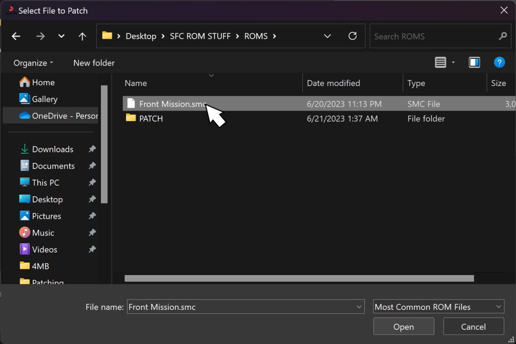
While you can use an online tool through your web browser, I recommend using the ‘Lunar IPS‘ utility. In this part of the tutorial I will be patching Front Mission and will be using the ‘mteam’ fan translation patch to address the issues found in the ‘F.H’ patch. However, before applying the mteam patch, I’ll need to have an unheadered Front Mission ROM that is already patched with the English translation v1.0b by F.H. You can download the F.H patch from here and the mteam addendum patch from here.
If you dumped a decrypted ROM using a CFW Retron5, it should already be headerless. To confirm, you can use ucon64 to check if the ROM has a header. If it does have a header, you can follow the methods described in section 2.2 to remove it. Once you have a headerless ROM, install Lunar IPS and download the patches.
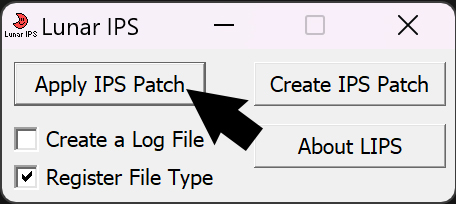
With Lunar IPS installed, simply double-click on the patch (IPS) file. This action will open a file explorer window. Navigate to the location where the Front Mission ROM file is stored within the file explorer. Select the ROM file, and the patch will be applied. However, in this tutorial, I will guide you through the process of using the Lunar IPS application specifically. We will begin with the F.H patch.
1. Launch Lunar IPS and click Apply IPS Patch
2. Select the patch (IPS) file.
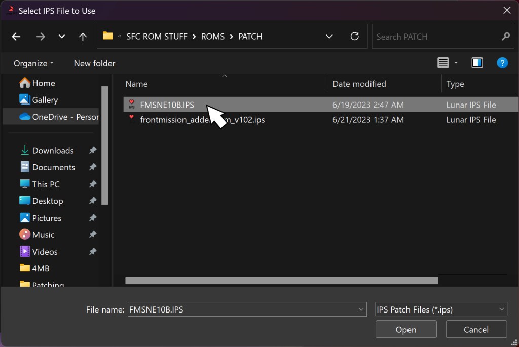
3. Select ROM, then hit “OK”. Patching Complete.
Now that we have an unheadered Front Mission ROM patched with the English translation v1.0b by F.H., we can proceed to apply the mteam patch and obtain a wonderfully translated Front Mission ROM. Before moving on to the next step of programming the EEPROM, it is crucial to check the integrity of the ROM using ucon64 and ensure that the checksums are correct. if you require assistance with ucon64 or need to fix the checksums, please refer to the process outlined in section 2.2, also if you need to split a ROM to accommodate a PCB with two Mask ROMs, I will show you how in the next subsection.
2.4 Splitting a ROM
Rom splitting involves dividing a single ROM file into multiple smaller files. This technique is used when dealing with game cartridges that contain two Mask ROMs. To perform the split, you can use specialized software like SNES ROM Utility, which allows you to specify the desired split size.
After splitting the ROM, you will end up with several smaller files, each containing a portion of the original game data. These files can then be programmed onto a EEPROM. It’s important to note that the files are labeled numerically, with the number 1 file intended for the first Mask ROM (the bottom one).
Here’s a step-by-step guide to splitting a ROM in SNES ROM Utility:
1. After you launch the SNES ROM Utility application look for the “Split File” option.
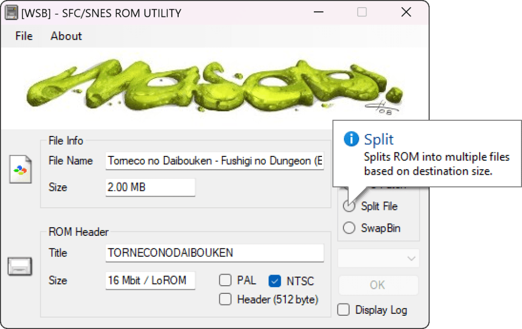
2. Click on the drop down menu. Depending on the size of the ROM, you may see different splitting sizes. Choose the option that splits the file into halves. For example, if you have a 4MB ROM, select the option to split it into two 2MB halves. If you have a 2MB ROM, choose the option to split it into two 1MB halves, and so on.
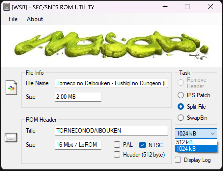
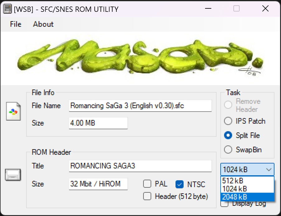
3. After selecting the appropriate halve size, click “OK” or a similar button to initiate the splitting process. The application will create two separate files, effectively splitting the ROM into two halves.

Section 3: Programming the EEPROM
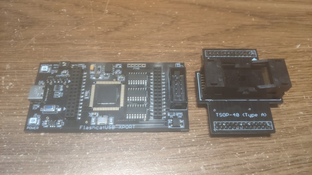
In this section, I will guide you through the process of programming an EEPROM using the FlashcatUSB XPORT by embedded computers. With the help of the TSOP-40 (Type-A) adapter I will demonstrate how to use the FlashcatUSB software to write the newly translated Front Mission ROM onto an M29F033 EEPROM, but the porcess is the same with the AM29F016. Just be advise you will need the TSOP-48 (NOR X8) adapter for the AM29F016 EEPROM
Programming the EEPROM is a crucial step, as it allows us to transfer the modified ROM data onto a physical chip that can be used in compatible hardware. By following the steps outlined in this section, you will gain valuable insights into the FlashcatUSB XPORT and learn how to utilize the FlashcatUSB software.

The FlashcatUSB XPORT is an excellent and cost-effective solution for programming a wide range of EEPROMs. It is regularly updated to enhance compatibility with an expanding list of integrated circuits. You can find a comprehensive list of supported chips on the embedded computers website. For this section of the tutorial, I will provide links to the FlashcatUSB XPORT programmer, TSOP-40 (Type-A), and the TSOP-48 (NOR X8) adapters required to program the M29F033 and AM29F016 chips.
Here are the recommended tools for this section:
- FlashcatUSB XPORT – This versatile programmer offers extensive compatibility and is highly recommended for EEPROM programming.
- TSOP-40 (Type-A) Adapter – The TSOP adapter is used for programming the M29F033 chip.
- TSOP-48 (NOR X8) Adapter – The TSOP adapter is used for programming the AM29F016 chip.
With these tools, we can proceed to the next steps of the tutorial, where I will guide you through using the FlashcatUSB software to program the freshly translated Front Mission ROM onto a M29F033 EEPROM.
3.1 FlashcatUSB software
While I won’t be providing a step-by-step walkthrough for installing the FlashcatUSB software and its drivers, I will direct you to the embedded computers website where you can download FlashcatUSB. The download package includes a comprehensive manual that provides instructions for driver installation and offers an overview of the software. It is important to follow the manual carefully to ensure proper installation and usage.
Once you have successfully installed the software, we can proceed to the next section where I will guide you through the process of programming the EEPROM.
3.2 Programming the EEPROM
When working with an adapter and an EEPROM, it’s common to find markings such as dots or notches that help identify Pin One and ensure the correct orientation. Additionally, some adapters may have arrows to indicate the correct orientation when inserting them into the programmer. Here’s an explanation of these markings:
- Pin One Indicator:
- Adapter: The adapter will have a small dot one side, which serves as an indicator for Pin One. This marking helps you align the EEPROM correctly with the adapter.
- EEPROM: Similarly, the EEPROM chip itself will have polarity mark ( a small circle) to indicate the location of Pin One. It aligns with the corresponding indicator on the adapter.
When inserting the EEPROM into the adapter:
- Align the polarity mark on the EEPROM with the corresponding dot on the adapter. It’s worth noting that some EEPROMs may have their polarity mark located on the bottom of the chip, and occasionally there may be two marks, which can be confusing. Typically, the smaller circle represents the polarity mark.
- Arrows for Orientation:
- Adapter: The adapters will have two arrows to indicate the correct orientation when inserting them into the programmer. These arrows signify the direction in which the adapter should be oriented for proper connectivity.
- Programmer: The programmer has corresponding markings to guide you in aligning the adapter correctly.
When inserting the adapter into the programmer:
- Observe the arrows or markings on both the adapter and the programmer.
- Align the arrows on the adapter with the arrows on the programmer to ensure correct orientation.
To work with the M29F033 and AM29F016 EEPROMs, make sure to set the programmer to the appropriate voltage of 5V. Both EEPROMs are specifically designed to operate at this voltage.
After properly inserting the EEPROM into the programmer and ensuring the voltage is set to 5V, connect the programmer to your computer. The software will automatically detect the EEPROM. However, in case the EEPROM is not properly identified by the software, you can refer to the following:
- Verify the Orientation
- Check the Adapter Alignment
- Make sure legs of the IC are straight
- Voltage setting
- Review Settings (See below)
For the M29F033 chip we need to have these setting check.
- Verify Programming – This setting isn’t necessary but its useful. With this enabled it will add an additional step performed by the programmer to ensure that the data has been accurately and successfully written to the EEPROM.
During the verification process, the programmer reads back the data from the EEPROM immediately after writing it. It then compares this readback data with the original data that was intended to be written. If the two sets of data match, it indicates that the programming was successful and the data has been reliably stored in the EEPROM. On the other hand, if there is a mismatch between the readback data and the original data, it indicates a programming error or a problem with the EEPROM.
Enabling the verification process provides an extra level of confidence that the data has been correctly written to the EEPROM. It helps to detect any potential issues such as programming errors, faulty connections, or compatibility problems between the programmer and the EEPROM.
By performing the verification step, the programmer can alert the user if any errors or discrepancies are detected during the programming process. This allows the user to take corrective action, such as reprogramming the EEPROM or addressing any connection issues, to ensure the data integrity.
It’s worth noting that enabling the verification process may slightly increase the overall programming time, as the programmer needs to read back the data and compare it with the original data. However, this additional time is often considered worthwhile to ensure the reliability of the programming process.
Overall, enabling the verification process provides an important quality assurance step to confirm the accuracy of the data programmed into the EEPROM, enhancing the reliability of your programmed device or project. - Voltage – When working with the M29F033 and AM29F016 EEPROMs, it’s important to note that it operates at a voltage of 5V. To ensure proper operation and compatibility, it is necessary to check the voltage switch on the programmer and select the appropriate position. The voltage switch controls the output voltage of the programmer. When the switch is positioned to the right, the board will operate and output at 5V. Conversely, when the switch is positioned to the left, the board will operate and output at 3.3V.
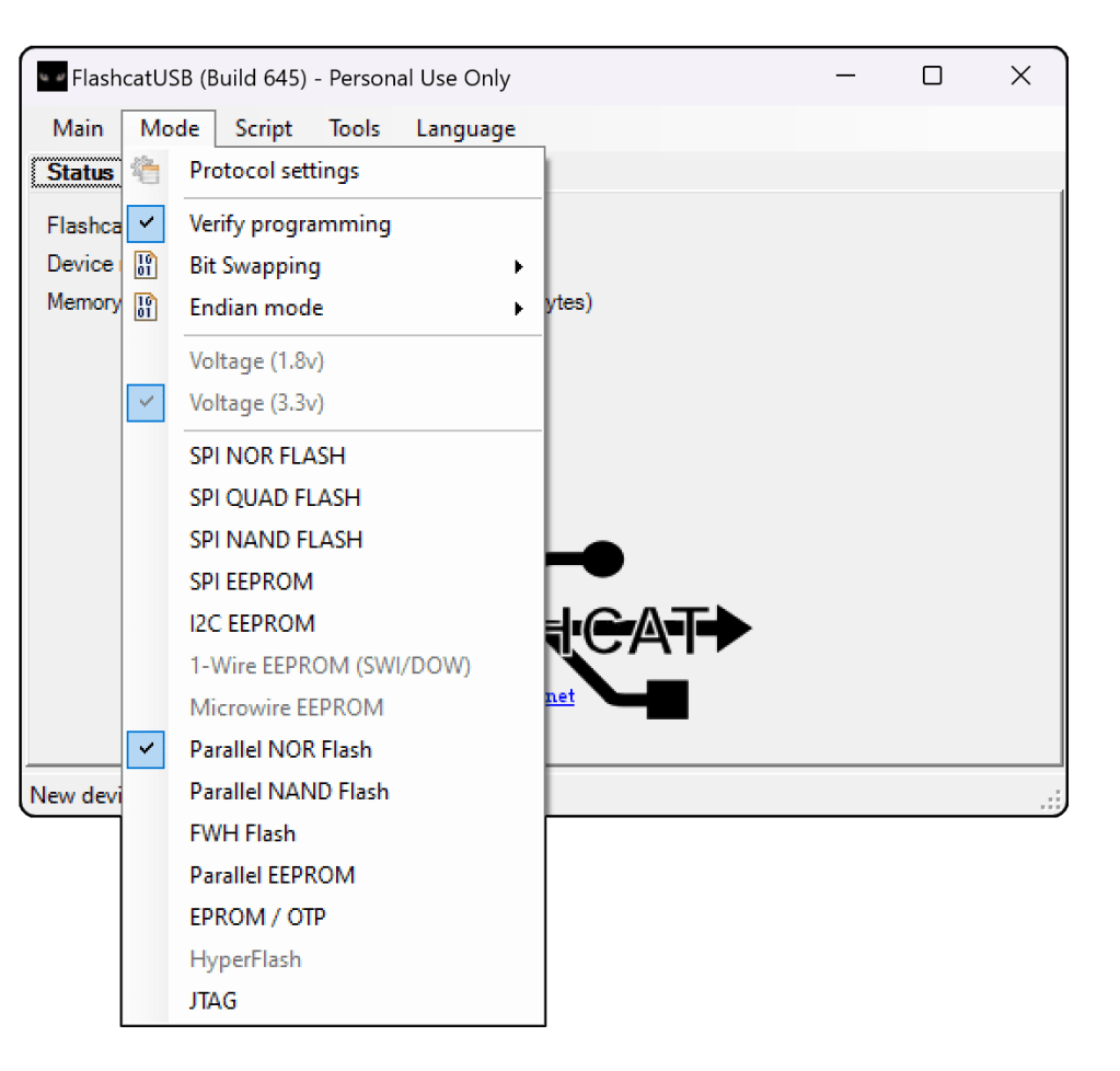
- Parallel NOR Flash – By choosing the “Parallel NOR Flash” setting, you are indicating to the software that you are working with a NOR flash memory device and you want to utilize the parallel programming mode for optimal performance.
If you’re still having problems with the EEPROM being recognized, there are a few other factors to consider. It’s important to pay attention to the condition of the EEPROMS’s legs. Even slight bends in the legs can interfere with the programmer’s ability to read the EEPROM correctly. Therefore, it is crucial to ensure that the legs of the chip are straight and in good condition. Additionally, the EEPROMs we are using for ROM programming, such as the M29F033 and AM29F016 chips, are relatively old and have been in circulation for decades. This means there is a chance of getting a faulty chip. Faulty chips can result from factors like age, mishandling, or environmental conditions, which may prevent the programmer from recognizing or write to the EEPROM. To minimize this risk, it is recommended to order multiple chips whenever possible. Having backups available can be helpful in case you encounter a faulty chip.
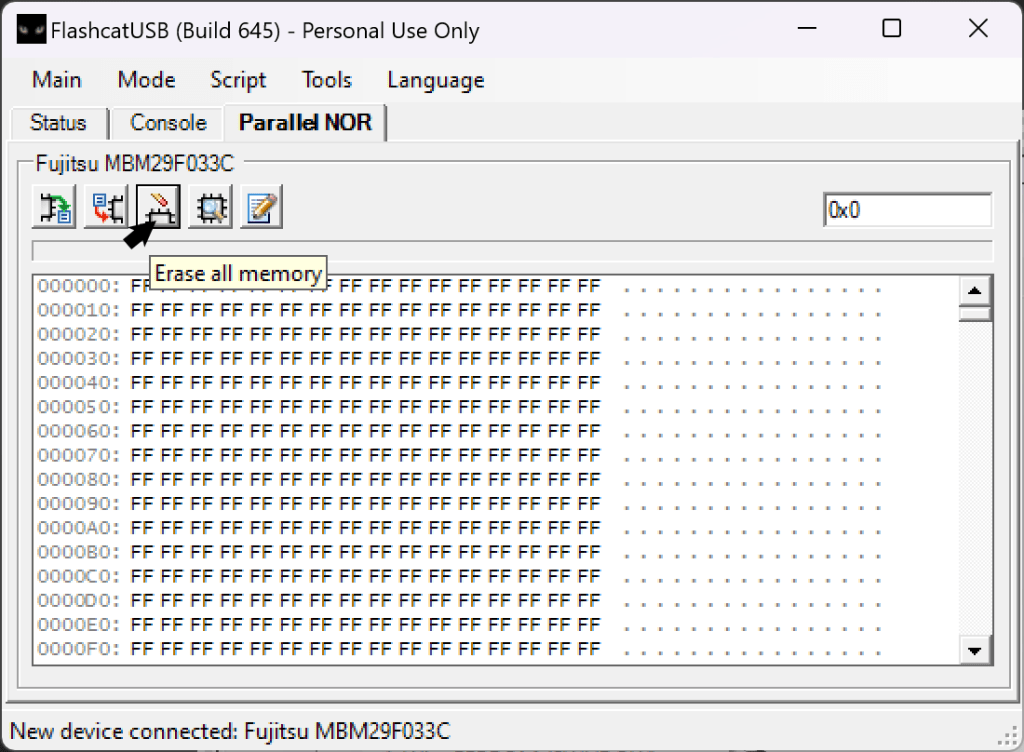
Before proceeding with programming, it is important to clear the EEPROM of any existing data. This step ensures a clean slate and avoids any potential conflicts or remnants from previous programming.
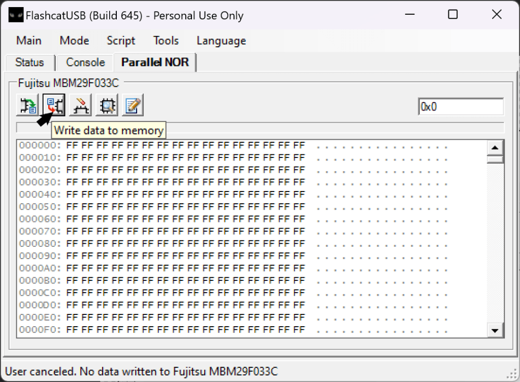
To clear the EEPROM, navigate to the ‘Parallel NOR’ tab in the FlashcatUSB software. In this tab, you will find five buttons located above the ‘Hex view’. Click on the third button, as shown in the image below. This action will erase all the memory contents of the EEPROM.
Now we are ready to write the ROM to the EEPROM. To do this, click on the ‘Write’ button, as shown below. It will open the file explorer, allowing you to navigate to the folder where your patched ROM is located. However, it’s important to note that by default, the file explorer will be looking for .bin files. In this particular case, we are not working with that file format, so your SNES/SFC ROMs may not appear initially. To resolve this, click on the drop-down menu located at the bottom right of the screen and select “All files.” This will ensure that all file types are visible, including your SNES/SFC ROMs.

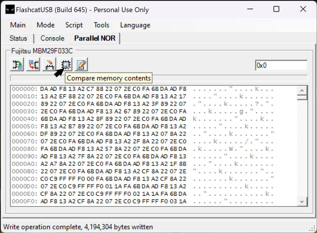
3.3 Verifying the Programmed ROM
After completing the writing process, it’s always a good idea to verify the programming to ensure accuracy. To do this, we will compare the contents of the EEPROM with the patched file. The programmer will perform the comparison and display the similarity as a percentage. Ideally, we want the EEPROM to be a 100% match with the file.
To initiate the comparison, click on the button shown below. Similar to when selecting the ROM during the writing process, we will select the file again. Once the comparison process is complete, a prompt will appear indicating the mismatch count. We want this count to be zero, indicating a perfect match.
If the comparison shows any amount of mismatch, it is recommended to erase the EEPROM and perform the writing process again. If the issue persists, ensure that the EEPROM is properly seated in the adapter. In my experience, even a slight bent leg can cause the compare test to fail by a small margin, such as 1%.
By carefully following these steps and ensuring a 100% match during the comparison, you can ensure the accurate programming of the EEPROM.
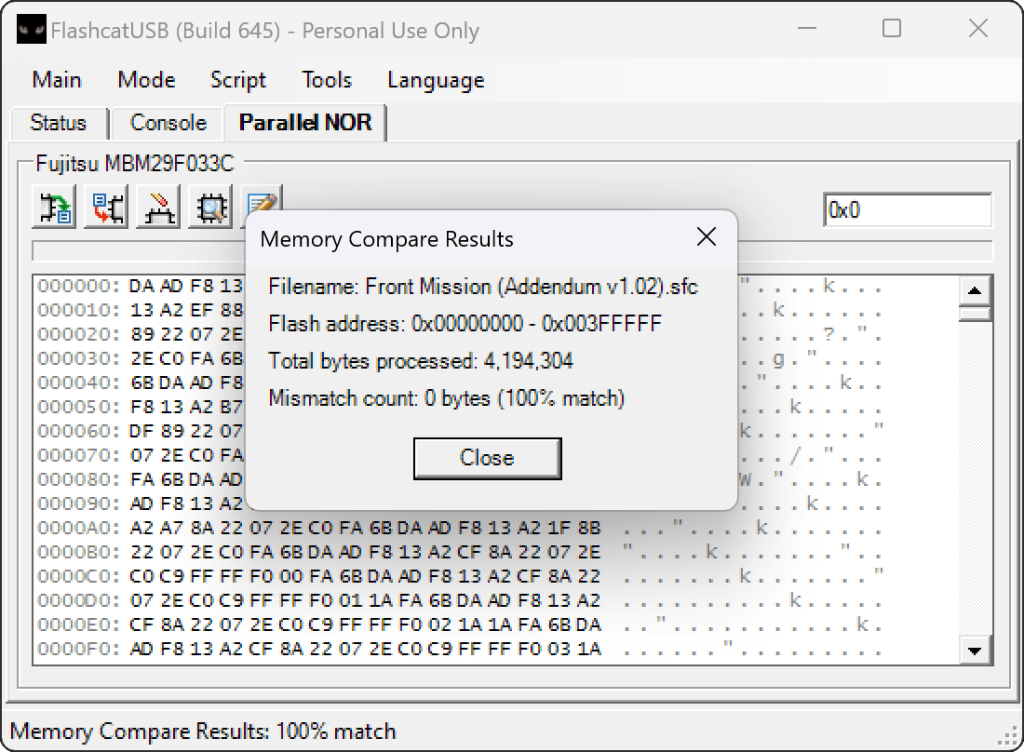
You have successfully programmed the EEPROM with your patched ROM. By verifying the programming and ensuring a 100% match, you can be confident in the accuracy of the data written to the EEPROM.
In the next section of the tutorial, we will explore how to disable the Mask ROM on the SNES cartridge so that we can install our newly programmed EEPROM. Disabling the Mask ROM will allow the system to read the data from the EEPROM instead of the original cartridge. It’s important to note that we will keep the original Mask ROM in circuit during this process, which ensures both game preservation and makes the modification fully reversible. This way, you can always revert to the original state if desired.
In the next sections, I will guide you through the process of disabling the Mask ROM and installing the newly programmed EEPROM into the SNES cartridge.
Section 4: Disabling the Factory MASKROM

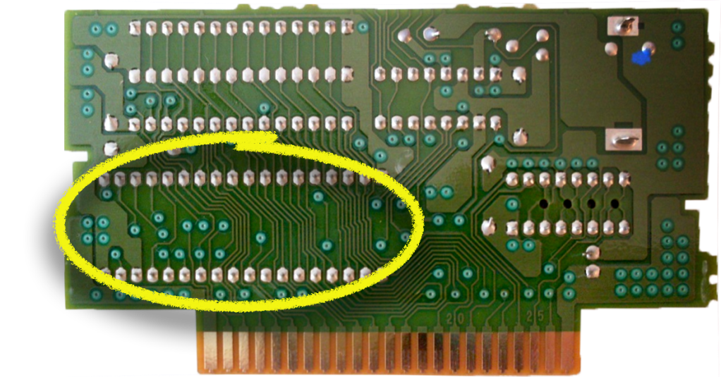
Inside a SNES game cartridge, you will find several different chips, each serving a specific purpose. For this tutorial, we will focus on the Mask ROM chip.
In some cases, you may come across SNES games that utilize two Mask ROM chips. The game’s data is split between the two chips. For instance, you might encounter a 4MB game that is divided into two 2MB Mask ROMs.
If you encounter such a scenario, where a game requires multiple Mask ROM chips, you will need two of my 2MB Snes Boogie Board adapters instead of a single 4MB board adapter. This ensures that each Mask ROM chip is properly accommodated.
It’s important to note that even for the same game title, there can be different revisions with varying PCB designs. Therefore, it is highly recommended to inspect your specific game board. By personally examining the PCB and identifying its unique characteristics, you can accurately determine the number and type of Mask ROM chips involved. To gather more information about the PCB of your cartridge, I recommend utilizing a helpful website called SNESCentral. This website serves as a database of SNES circuit boards and offers assistance in identifying the components on your game’s PCB. It will aid you in understanding the composition of your game cartridge’s PCB. This knowledge will greatly assist you in selecting the appropriate adapters.
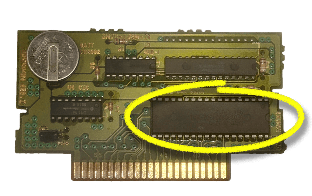
The Mask ROM has a CE (Chip Enable) pin that plays a crucial role in its operation. When the CE pin is pulled low (grounded), it enables the chip and allows it to function. This means that the ROM can be accessed and read by the system or other devices.
On the other hand, if the CE pin is driven high (connected to VCC or the supply voltage), it disables the chip. When the CE pin is high, the ROM becomes inactive and cannot be accessed or read. It essentially goes into a disabled state, preventing any data transfers or operations. In this section I will show you how to put the Mask ROM in a disabled state.
The CE pin on the Mask ROM is pulled low by default, which means it is connected to ground. In our modification process, we will intentionally disconnect the CE pin from the circuit and then connect it to the VCC instead. This reconfiguration will disable the ROM. In the image provided below, you can see the specific pins we will be working with. For a 32-pin Mask ROM, we will connect Pin 26 (CE) to Pin 36 (VCC), effectively tying them together. Similarly, for a 36-pin Mask ROM, we will connect Pin 24 (CE) to Pin 34 (VCC). NOTE: You could tie VCC to OE (Output Enable) instead. OE is pin 31 on the 32-pin ROM or pin 33 on the 36-pin ROM.
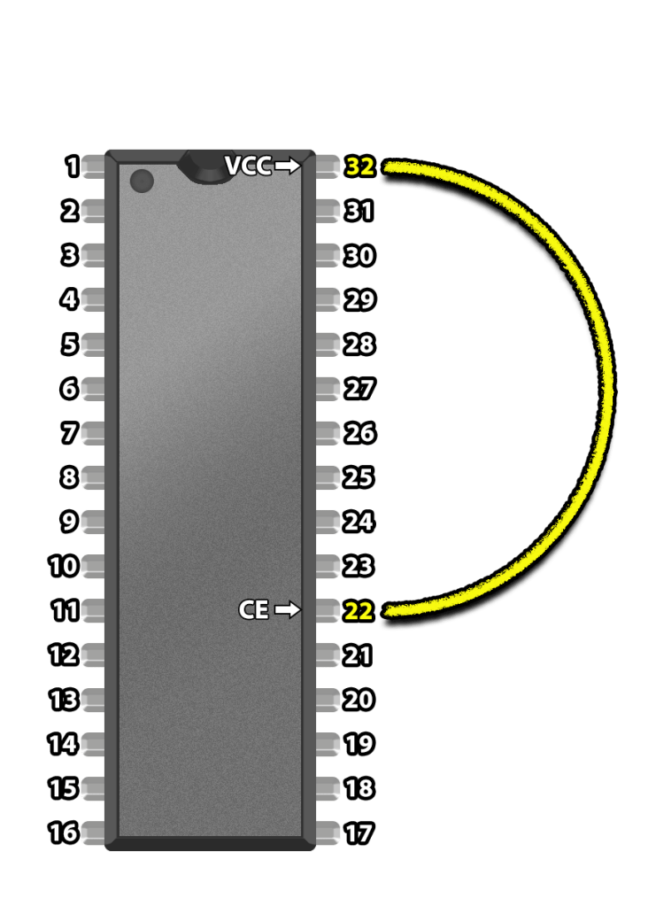

By making these connections, we are essentially overriding the default behavior of the CE pin and instructing the ROM chip to remain disabled. This alteration allows us to mount our EEPROM without removing the Mask ROM. The EEPROM will effectively take over the role of the ROM chip in providing the necessary data to the SNES system.
But before we tie anything together we first need to remove the CE pin from the Circuit.
Removing CE from the Circuit.
There are two methods available for removing the CE pin from the circuit, and both methods are reversible.
The first method involves using flush cuts or wire cutters to physically cut the CE pin from the board. By carefully cutting the pin, you can detach it from the circuit, effectively isolating it from the rest of the connections. Once cut, you can gently pull the leg of the pin away from the board, ensuring that it is no longer making contact with any traces or vias.
The second method, as shown in the provided images, involves desoldering the pin by removing the solder that connects it to the board. By applying heat to the solder joint and using a desoldering tool or solder wick, you can remove the solder and free the pin from its connection. With the solder removed, you can then use a small tool or tweezers to pry the pin out of the via (the hole in the PCB).

Wire CE (isolated) to VCC
Once the CE has been isolated and disconnected from the circuit, the next step is to establish a new connection to the appropriate VCC pin. In the provided example, where a 36-Pin Mask ROM is used, I will be wiring Pin 24 of the Mask ROM to Pin 34. To create this connection, I will be using Kynar 30 AWG wire

Section 5: Attaching the Boogie Board and Soldering the EEPROM
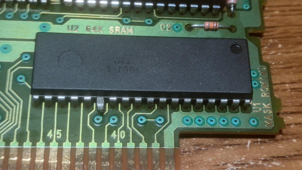
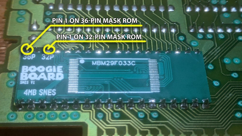
The Boogie Board mounts on the unpopulated side of the PCB, directly attaching it to the Mask ROM.
To begin, carefully align the pins of the Boogie Board with the corresponding pads on the PCB. Pay close attention to the alignment and make sure the pins are correctly matched with the pads. It’s important to note that the PCB has indicators for Pin 1, which is essential for proper alignment.
For a 36-Pin Mask ROM, you’ll find Pin 1 labeled as “36P” on the Boogie Board. Similarly, for a 32-Pin Mask ROM, Pin 1 is labeled as “32P”.
Once you have aligned the pins, proceed to solder each connection with care. Aim for reliable and sturdy solder joints, a secure connection for each pin is important for proper functionality.
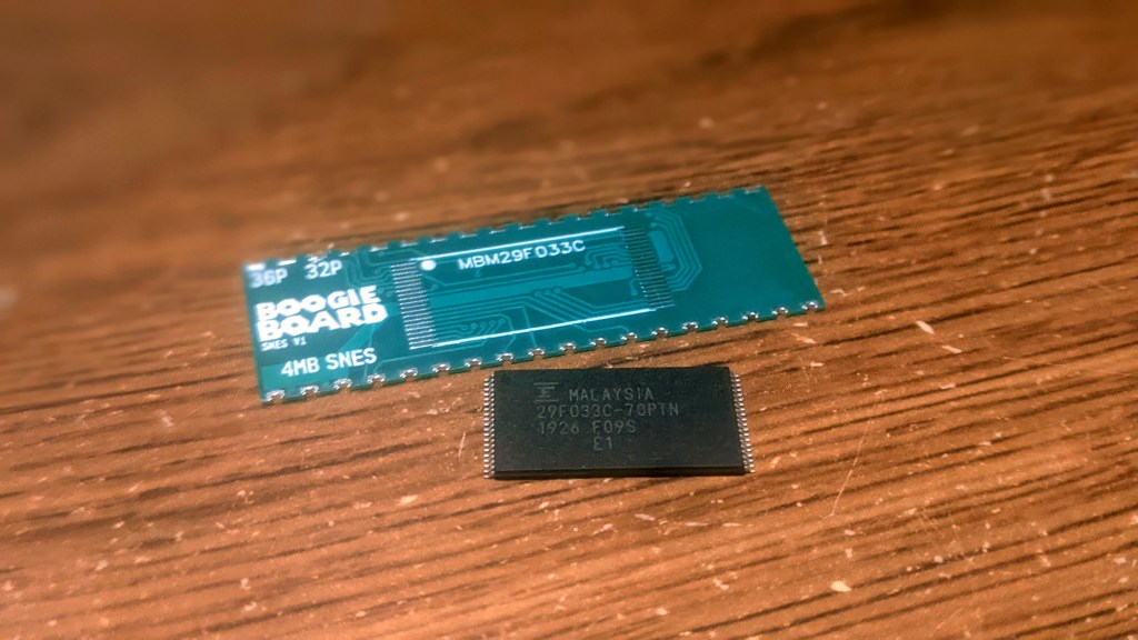
With the Boogie Board securely attached to the PCB, the next step is to solder the TSOP 40 or TSOP 48 EEPROM onto the board. Follow these steps to ensure a successful soldering process:
- Prepare the EEPROM: Ensure that the TSOP 40 or TSOP 48 EEPROM is ready for soldering. Check for any bent or misaligned pins and gently straighten them if needed. Double-check that you have the correct EEPROM for your specific board and configuration.
- Positioning the EEPROM: Carefully align the pins of the EEPROM with the corresponding pads on the Boogie Board. Take your time to ensure precise alignment. Pay close attention to Pin 1, which is indicated by a dot on the corner of the EEPROM chip. Additionally, on the Boogie Board, there will be a corresponding dot to identify Pin 1. Align these dots to ensure the correct orientation of the EEPROM. Double-check the alignment before proceeding to the soldering step.
- Soldering the EEPROM: Once the EEPROM is properly positioned, solder each pin individually. Start with one corner pin to hold the EEPROM in place. Apply a small amount of solder to the tip of your soldering iron, then heat the pad and pin simultaneously for a few seconds until the solder flows and creates a solid connection. Repeat this process for the remaining pins, working your way across the chip.
- Inspect: After soldering, visually inspect the solder joints to ensure they are smooth, shiny, and free from any bridges or cold joints. Use a magnifying glass if necessary. Once you are satisfied with the soldering.
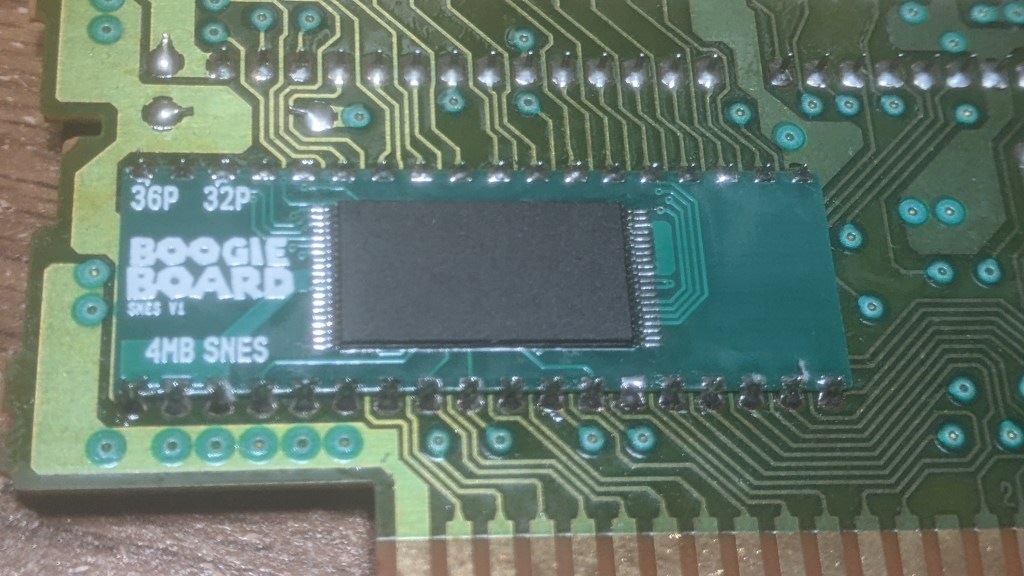
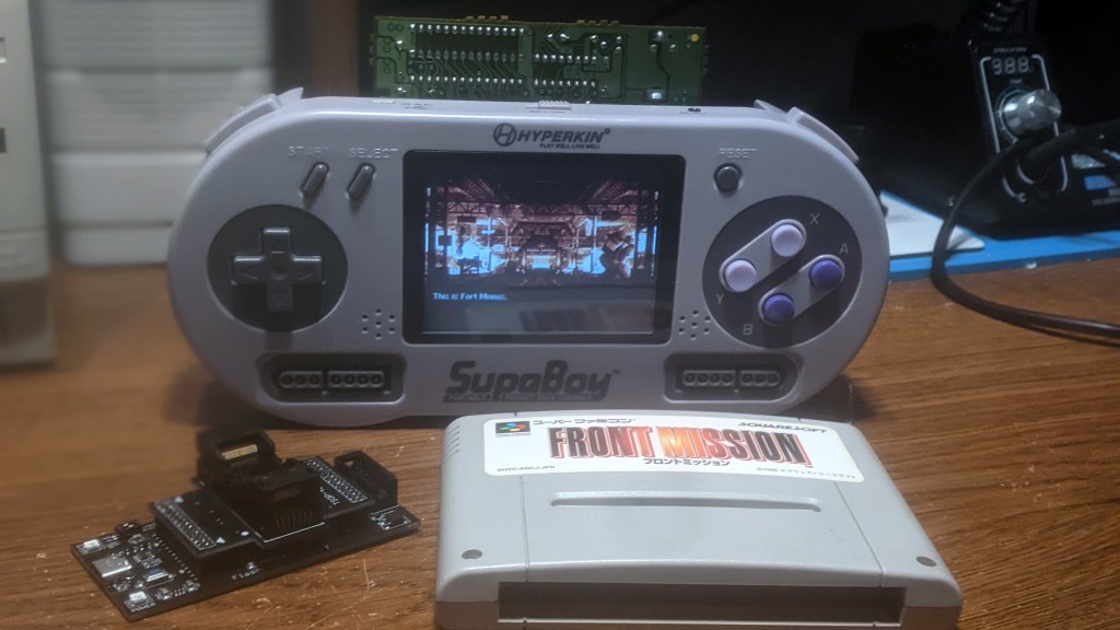
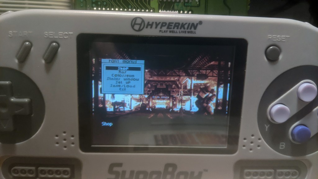
With the Boogie Board and EEPROM securely soldered in place, you have completed the hardware modifications. Now it’s time to test the game cartridge by powering on your SNES console. If the game boots up correctly, congratulations! You have successfully modified and translated your SNES game cartridge.

In the event that you encounter any issues booting the game, don’t worry. I have prepared a troubleshooting section in the next part of this tutorial. It will provide you brief instructions to help diagnose and resolve common issues.
Proceed to the next section, where I will address troubleshooting techniques and offer solutions to some of the issues you may encounter.
Section 6: Troubleshooting and Tips
If the game fails to boot up after soldering the EEPROM onto the Boogie Board, there are a few thing you should double check. I’ll start with the most common issues.
- Check the soldering on the EEPROM: Take a close look at the solder joints connecting the EEPROM and the Boogie Board. It’s easy to miss a pin or have unintentional solder bridges. To ensure a reliable connection, I recommend using an eye loupe or magnifying glass to inspect the joints. Look for any bridges where solder may have inadvertently connected two pins together. If you don’t see any bridges, you can reapply a small amount of solder and carefully sweep across the pins, paying extra attention to the corner pins of the IC, as they are easily missed. Once you’ve done this, double-check for any remaining bridges. This step is crucial as it addresses the most common issue encountered during the modification process.
- Check the soldering on the Boogie Board: Take a careful look at all the connections on the board that correspond to the Mask ROM. It’s important to note that since we removed the CE pin, the Boogie Board doesn’t have a leg to be soldered on that specific pad. This particular pad can be prone to mistakes, so pay extra attention to ensure proper soldering. Double-check this connection to ensure it is secure and accurately soldered.
- Verify the alignment: Double-check the alignment of the EEPROM and Boogie Board. Ensure that Pin 1 is correctly positioned, as described earlier. Misalignment can cause connection issues and prevent the game from functioning properly.
- Confirm the patch ROM: Verify that the ROM file is correctly patched and compatible with the game cartridge. Recheck the steps to ensure that the ROM is error-free.
If the game boots up but fails shortly after, there are some potential causes to consider.
- Upper Address pins: If you’re using a 4MB Boogie Board on a 32-Pin Mask ROM, it’s possible that the higher address pins on the EEPROM are not being accessed. Some game PCBs have vias designed for a 36-Pin Mask ROM even when equipped with a 32-Pin one. When using a fully programmed 4MB EEPROM you might to make connections on the Boogie Board to these vias. These pads correspond to pins 1, 2, 34, and 36 on the 36-Pin Mask ROM.
- Copy protection or specific size requirements: Certain ROMs may have copy protection mechanisms or specific size requirements. For example, as mentioned before with FF5, the ROM might expect mirroring or a specific size.
